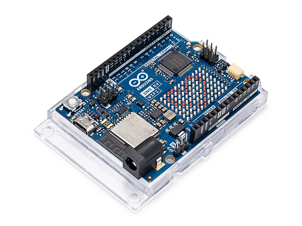
Arduino Uno R4 Wifi
1. Description
The Arduino UNO R4 WiFi (hereafter for UNO R4 WiFi) is the first UNO board to feature a 32-bit microcontroller and an ESP32-S3 Wi-Fi®module (ESP32-S3-MINI-1-N8). It features a RA4M1 series microcontroller from Renesas (R7FA4M1AB3CFM#AA0), based on a 48 MHz Arm® Cortex®-M4 microprocessor.
The board features 14 digital I/O ports, 6 analog channels, dedicated pins for I2C, SPI and UART connections. It has a significantly larger memory: 8 times more flash memory (256 kB) and 16 times more SRAM (32 kB). With a 48 MHz clock speed, it is also 3x faster than its predecessors.
In addition, it features an ESP32-S3 module for Wi-Fi® & Bluetooth® connectivity, as well as a built-in 12×8 LED matrix, making it one of the most visually unique Arduino boards to date. The LED matrix is fully programmable, where you can load anything from still frames to custom animations.
The RA4M1’s operating voltage is fixed at 5 V, whereas the ESP32-S3 module is 3.3 V. Communication between these two MCUs is performed via a logic-level translator (TXB0108DQSR).
2,000 L
1. Description
The Arduino UNO R4 WiFi (hereafter for UNO R4 WiFi) is the first UNO board to feature a 32-bit microcontroller and an ESP32-S3 Wi-Fi®module (ESP32-S3-MINI-1-N8). It features a RA4M1 series microcontroller from Renesas (R7FA4M1AB3CFM#AA0), based on a 48 MHz Arm® Cortex®-M4 microprocessor.
The board features 14 digital I/O ports, 6 analog channels, dedicated pins for I2C, SPI and UART connections. It has a significantly larger memory: 8 times more flash memory (256 kB) and 16 times more SRAM (32 kB). With a 48 MHz clock speed, it is also 3x faster than its predecessors.
In addition, it features an ESP32-S3 module for Wi-Fi® & Bluetooth® connectivity, as well as a built-in 12×8 LED matrix, making it one of the most visually unique Arduino boards to date. The LED matrix is fully programmable, where you can load anything from still frames to custom animations.
The RA4M1’s operating voltage is fixed at 5 V, whereas the ESP32-S3 module is 3.3 V. Communication between these two MCUs is performed via a logic-level translator (TXB0108DQSR).
2. Features
R7FA4M1AB3CFM#AA0, also called RA4M1, is the main MCU on UNO R4 WiFi board, which connects to all pins on the board and all communication buses.
Overview
48 MHz Arm® Cortex®-M4 microprocessor with a floating point unit (FPU)
5 V operating voltage
Real-time Clock (RTC)
Memory Protection Unit (MPU)
Digital Analog Converter (DAC)
Memory
256 kB Flash Memory
32kB SRAM
8 kB Data Memory (EEPROM)
Peripherals
Capacitive Touch Sensing Unit (CTSU)
USB 2.0 Full-Speed Module (USBFS)
14-bit ADC
up to 12-bit DAC
Operational Amplifier (OPAMP)
Power
RA4M1 operating voltage is 5V
Recommended input voltage (VIN) is 6-24 V
Barrel jack connected to VIN pin (6-24V)
Power via USB-C® at 5 V
Communication
1x UART (pin D0, D1)
1x SPI (pin D10-D13, ICSP header)
1x I2C (pin A4, A5, SDA, SCL)
1x CAN (pin D4, D5, external transceiver is required)
Operating temperature: -40℃~85℃
esp32 – s3 mini -1- n8 is a secondary MCU with a built-in antenna for Wi-Fi® and Bluetooth® connection. This module works at 3.3V, and communicates with RA4M1 through a logical level translator (TXB0108DQSR).
Overview
Xtensa® Dual-core 32-bit LX7 microprocessor
Operating voltage of 3.3V
40 MHz crystal oscillator
Wi-Fi®
Wi-Fi® supports 802.11 b/g/n standard (Wi-Fi®4)
Bit rate up to 150 Mbps
Frequency band of 2.4 GHz
Bluetooth®
Bluetooth® 5
3. Functions
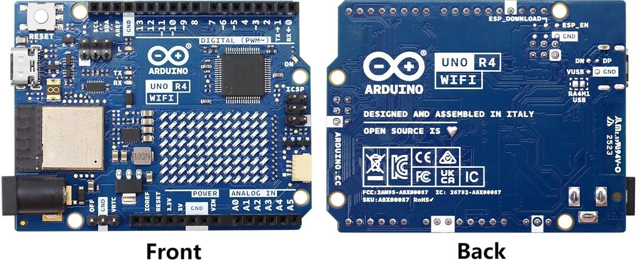
3.1. Board Topology
Img
Ref.
Description
U1
R7FA4M1AB3CFM#AA0 Microcontroller IC
U2
NLASB3157DFT2G multiplexer
U3
ISL854102FRZ-T Buck converter
U4
TXB0108DQSR Logic level converter(5 V – 3.3 V)
U5
SGM2205-3.3XKC3G/TR 3.3 V Linear voltage regulator
U6
NLASB3157DFT2G multiplexer
U_LEDMATRIX
12×8 LED red matrix
M1
ESP32-S3-MINI-1-N8
PB1
RESET button
JANALOG
Analog input/output headers
JDIGITAL
Digital input/output headers
JOFF
OFF, VRTC headers
J1
CX90B-16P USB-C® connector
J2
SM04B-SRSS-TB(LF)(SN) I2C connector
J3
ICSP headers (SPI)
J5
DC power jack
J6
ESP headers
DL1
LED TX (serial transmit)
DL2
LED RX (serial receive)
DL3
LED Power (green)
DL4
LED SCK (serial clock)
D1
PMEG6020AELRX Schottky Diode
D2
PMEG6020AELRX Schottky Diode
D3
PRTR5V0U2X, 215 ESD Protection
3.2. Microcontroller (R7FA4M1AB3CFM#AA0)
The UNO R4 WiFi is based on the 32-bit RA4M1 series microcontroller, R7FA4M1AB3CFM#AA0, from Renesas, which uses a 48 MHz Arm® Cortex®-M4 microprocessor with a floating point unit (FPU).
On the board, the operating voltage is fixed at 5 V to be fully retro compatible with shields, accessories & circuits originally designed for older UNO revisions.
The R7FA4M1AB3CFM#AA0 features:
256 kB flash / 32 kB SRAM / 8 kB data flash (EEPROM)
Real-time Clock (RTC)
4x Direct Memory Access Controller (DMAC)
up to 14-bit ADC
up to 12-bit DAC
OPAMP
1x CAN bus
3.3. Wi-Fi® / Bluetooth® Module (ESP32-S3-MINI-1-N8)
The Wi-Fi® / Bluetooth® LE module on the UNO R4 WiFi is from the ESP32-S3 SoCs. It features the Xtensa® dual-core 32-bit LX7 MCU, a built-in antenna and support for 2.4 GHz bands.
The ESP32-S3-MINI-1-N8 features:
Wi-Fi® 4 – 2.4 GHz band
Bluetooth® 5 LE support
3.3 V operating voltage
384 kB ROM
512 kB SRAM
Up to 150 Mbps bit rate
This module acts as a secondary MCU on the UNO R4 WiFi, and communicates with the RA4M1 MCU using a logic-level translator. Note that this module operates on 3.3 V as opposed to the RA4M1’s 5 V operating voltage.
3.4. ESP Header
Img
The header located close to the RESET button can be used to access the ESP32-S3 module directly. The pins accessible are:
ESP_IO42 – MTMS debugging (Pin 1)
ESP_IO41 – MTDI debugging (Pin 2)
ESP_TXD0 – Serial Transmit (UART) (Pin 3)
ESP_DOWNLOAD – boot (Pin 4)
ESP_RXD0 – Serial Receive (UART) (Pin 5)
GND – ground (Pin 6)
Img
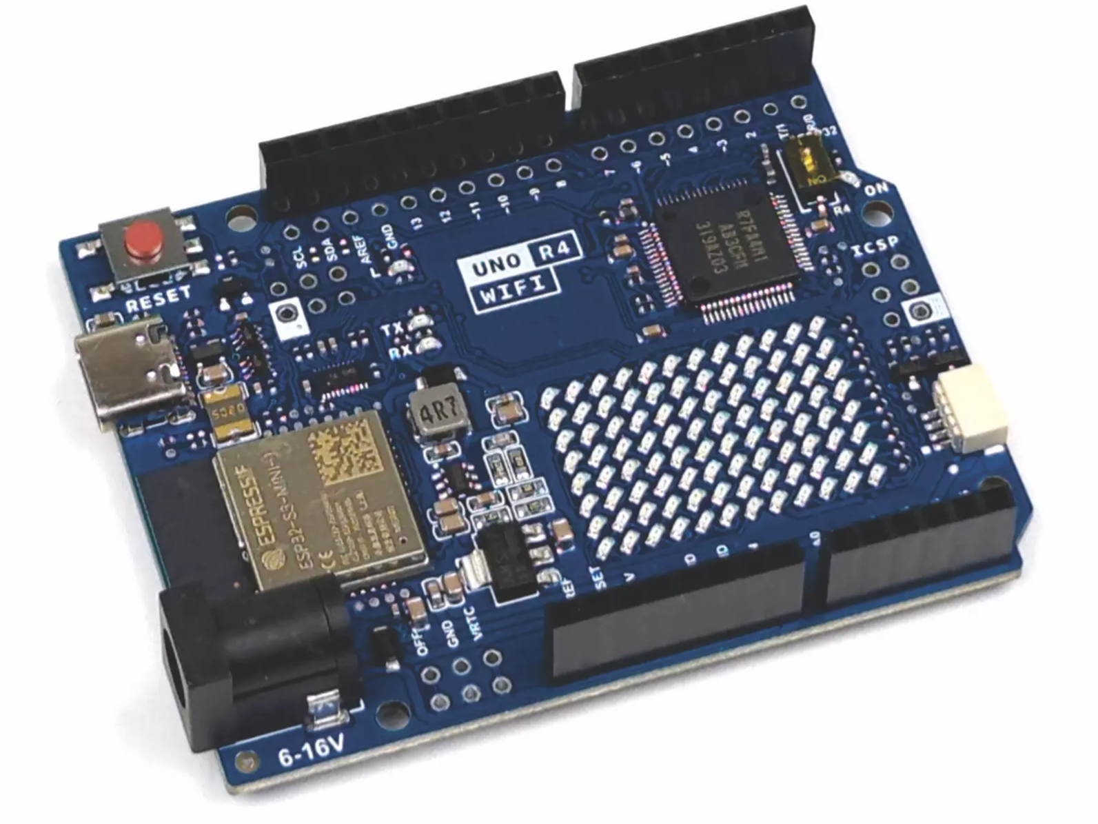
3.5. USB Bridge
When programming the UNO R4 WiFi, the RA4M1 MCU is programmed via the ESP32-S3 module by default. The U2 and U6 switches can switch the USB communication to go directly to the RA4M1 MCU, by writing a high state to the P408 pin (D40).
Img
Soldering together the SJ1 pads permanently sets the USB communication directly to the RA4M1, bypassing the ESP32-S3.
3.6. USB Connector
The UNO R4 WiFi has one USB-C® port, used to power and program your board as well as sending & receiving serial communication.
NOTE: The board should not be powered with more than 5 V via the USB-C® port.
3.7. LED Matrix
The UNO R4 WiFi features a 12×8 matrix of red LEDs (U_LEDMATRIX), connected using the technique known as charlieplexing. The following pins on the RA4M1 MCU are used for the matrix:
P003
P004
P011
P012
P013
P015
P204
P205
P206
P212
P213
Img
These LEDs can be accessed as an array, using a specific library. See the mapping below:
Img
This matrix can be used for a number of projects and prototyping purposes, and supports animation, simple game designs and scrolling text among other things.
3.8. Digital Analog Converter (DAC)
The UNO R4 WiFi has a DAC with up to 12-bit resolution attached to the A0 analog pin. A DAC is used to convert a digital signal to an analog signal.
The DAC can be used for signal generation for e.g. audio applications, like generating and altering sawtooth waves.
3.9. I2C Connector
The I2C connector SM04B-SRSS-TB(LF)(SN) is connected to a secondary I2C bus on the board.
Note that this connector is powered via 3.3 V.
Img
This connector also shares the following pin connections:
JANALOG headers
A4
A5
JDIGITAL headers
SDA
SCL
NOTE: as A4/A5 is connected to the main I2C bus, these should not be used as ADC inputs whenever the bus is in use. You can however connect I2C devices to each of these pins and connectors simultaneously.
3.10. Power Options
Power can either be supplied via the VIN pin, or via USB-C® connector. If power is supplied via VIN, the ISL854102FRZ buck converter steps the voltage down to 5 V.
Both VUSB and VIN pins are connected to the ISL854102FRZ buck converter, with Schottky diodes in place for reverse polarity & overvoltage protection respectively.
Power via USB supplies about ~4.7 V (due to Schottky drop) to the RA4M1 MCU.
The linear regulator (SGM2205-3.3XKC3G/TR) converts 5 V from either the buck converter or USB, and provides 3.3V to a number of components, including the ESP32-S3 module.
Power Tree
Img
Pin Voltage
The general operating voltage for UNO R4 WiFi is 5 V, however the ESP32-S3 module’s operating voltage is 3.3 V.
NOTE: It is very important that ESP32-S3’s pins (3.3 V) do not come in contact with any of the RA4M1’s pins (5 V), as this may damage the circuits.
Pin Current
The GPIOs on the R7FA4M1AB3CFM#AA0 microcontroller can safely handle up to 8 mA of current. Never connect devices that draw higher current directly to a GPIO as this may damage the circuit.
For powering e.g. servo motors, always use an external power supply.
4. Pin-out
Img
Img
4.1. Analog
Pin
Function
Type
Description
1
BOOT
NC
Not Connected
2
IOREF
IOREF
Reference for digital logic V – connected to 5 V
3
Reset
Reset
Reset
4
+3V3
Power
+3V3 Power Rail
5
+5V
Power
+5V Power Rail
6
GND
Power
Ground
7
GND
Power
Ground
8
VIN
Power
Voltage Input
9
A0
Analog
Analog input 0 / DAC
10
A1
Analog
Analog input 1 / OPAMP+
11
A2
Analog
Analog input 2 / OPAMP-
12
A3
Analog
Analog input 3 / OPAMPOut
13
A4
Analog
Analog input 4 / I2C Serial Datal (SDA)
14
A5
Analog
Analog input 5 / I2C Serial Clock (SCL)
4.2. Digital
Pin
Function
Type
Description
1
SCL
Digital
I2C Serial Clock (SCL)
2
SDA
Digital
I2C Serial Datal (SDA)
3
AREF
Digital
Analog Reference Voltage
4
GND
Power
ground
5
D13/SCK/CANRX0
Digital
GPIO 13 / SPI Clock / CAN Receiver (RX)
6
D12/CIPO
Digital
GPIO 12 / SPI Controller In Peripheral Out
7
D11/COPI
Digital
GPIO 11 (PWM) / SPI Controller Out Peripheral In
8
D10/CS/CANTX0
Digital
GPIO 10 (PWM) / SPI Chip Select / CAN Transmitter (TX)
9
D9
Digital
GPIO 9 (PWM~)
10
D8
Digital
GPIO 8
11
D7
Digital
GPIO 7
12
D6
Digital
GPIO 6 (PWM~)
13
D5
Digital
GPIO 5 (PWM~)
14
D4
Digital
GPIO 4
15
D3
Digital
GPIO 3 (PWM~) / Interrupt Pin
16
D2
Digital
GPIO 2 / Interrupt Pin
17
D1/TX0
Digital
GPIO 1 / Serial 0 Transmitter (TX)
18
D0/TX0
Digital
GPIO 0 / Serial 0 Receiver (RX)
4.3. OFF
Pin
Function
Type
Description
1
OFF
Power
For controlling power supply
2
GND
Power
Ground
1
VRTC
Power
Battery connection to power RTC only
4.4. ICSP
Pin
Function
Type
Description
1
CIPO
Internal
Controller In Peripheral Out
2
+5V
Internal
5V Power
3
SCK
Internal
Serial Clock
4
COPI
Internal
Controller Out Peripheral In
5
RESET
Internal
Reset
6
GND
Internal
Ground
For more information of UNO R4 WiFi board, please visit: https://docs.arduino.cc/hardware/uno-r4-wifi/
Ⅱ. UNO R4 Minima Board
Img
1. Description
The Arduino® UNO R4 Minima is the first UNO board to feature a 32-bit microcontroller. It features a RA4M1 series microcontroller from Renesas (R7FA4M1AB3CFM#AA0), which embeds a 48 MHz Arm® Cortex®-M4 microprocessor.
The board features the standard 14 digital I/O ports, 6 analog channels, dedicated pins for I2C, SPI and UART connections. Compared to its predecessors the board has a much larger memory: 8 times more flash memory (256 kB) and 16 times more SRAM (32 kB) as well as 8 kB data memory (EEPROM).
has a barrel jack connector and supports input voltages from 6-24 V. This connector is widely popular and removes the need for additional circuitry required to step down the voltage.
The UNO R4 Minima board’s operating voltage is 5 V, making it hardware compatible with UNO form factor accessories with the same operating voltage. Shields designed for previous UNO revisions are therefore safe to use with this board but are not guaranteed to be software compatible due to the change of microcontroller.
2. Features
R7FA4M1AB3CFM#AA0
48 MHz Arm® Cortex®-M4 microprocessor with a floating point unit (FPU).
5V operating voltage
Real-time Clock (RTC)
Memory Protection Unit (MPU)
Digital-to-analog Converter (DAC)
Memory
256kB flash memory
32kB SRAM
8 kB Data Memory (EEPROM)
Header
14 digital I/O pins (GPIO), D0-D13
6 analog input pins (ADC), A0-A5
6 PWM pins: D3, D5, D6, D9, D10, D11
Peripherals
Capacitive Touch Sensing Unit (CTSU)
USB 2.0 Full-Speed Module (USBFS)
Up to 14-bit ADC
Up to 12-bit DAC
Operational Amplifier (OPAMP)
Power
Operating voltage is 5V
Recommended input voltage (VIN) is 6-24 V
Barrel jack connected to VIN pin (6-24 V)
Power via USB-C® at 5 V
Schottky diodes are used for over-voltage and reverse polarity protection
Communication
1x UART (D0, D1)
1x SPI (D10-D13, ICSP header)
1x I2C (A4, A5, SDA, SCL)
1x CAN (D4, D5, external transceiver is required)
Operating temperature: -40℃~85℃
3. Functions
3.1. Board Topology
Img
Ref.
Description
U1
R7FA4M1AB3CFM#AA0 Microcontroller IC
U2
ISL854102FRZ-T Buck Converter
PB1
RESET Button
JANALOG
Analog input/output headers
JDIGITAL
Digital input/output headers
J1
ICSP header (SPI)
J2
SWD/JTAG Connector
J3
CX90B-16P USB-C® Connector
J4
DC Jack
DL1
LED TX (serial transmit)
DL2
LED RX (serial receive)
DL3
LED Power (green)
DL4
LED SCK (serial clock)
D2
PMEG6020AELRX Schottky Diode
D3
PMEG6020AELRX Schottky Diode
D4
PRTR5V0U2X, 215 ESD Protection
3.2. Microcontroller (R7FA4M1AB3CFM#AA0)
The UNO R4 Minima is based on the 32-bit RA4M1 series microcontroller, R7FA4M1AB3CFM#AA0, from Renesas, which uses a 48 MHz Arm® Cortex®-M4 microprocessor with a floating point unit (FPU).
On the UNO R4 Minima, the operating voltage is fixed at 5 V to be fully retro compatible with shields, accessories & circuits originally designed for older UNO revisions.
The R7FA4M1AB3CFM#AA0 features:
256 kB flash / 32 kB SRAM / 8 kB data flash (EEPROM)
Real-time Clock (RTC)
4x Direct Memory Access Controller (DMAC)
up to 14-bit ADC
up to 12-bit DAC
OPAMP
CAN bus
3.3. USB Connector
The UNO R4 Minima has one USB-C® port, used to power and program your board as well as send & receive serial communication.
NOTE: You should not power the board with more than 5 V via the USB-C® port.
3.4. Digital Analog Converter (DAC)
The UNO R4 Minima has a DAC with up to 12-bit resolution attached to the A0 analog pin. A DAC is used to convert a digital signal to an analog signal.
3.5. Power Options
Power can either be supplied via the VIN pin, the barrel jack, or via USB-C® connector. If power is supplied via VIN, the ISL854102FRZ buck converter steps the voltage down to 5 V.
The VUSB, barrel jack connector and VIN pins are connected to the ISL854102FRZ buck converter, with Schottky diodes in place for reverse polarity & overvoltage protection respectively.
Power via USB supplies about ~4.7 V (due to Schottky drop) to the RA4M1 microcontroller.


There are no reviews yet.